DLI supported projects are scaling rapidly, with 16 tape-outs, 6 ASICs chips, 10 patents, 1,000+ engineers engaged, and over 3× private investment leveraged.
FinTech BizNews Service
Mumbai, 4 January 2026: India is rapidly advancing its semiconductor ambitions, recognizing semiconductor chips as critical enablers of healthcare, transport, communications, defence, space, and emerging digital infrastructure.
With accelerating digitalization and automation, global demand for semiconductor chips is rising sharply. In response, the Government of India, through the Semicon India Programme and the India Semiconductor Mission (ISM), is strengthening the domestic semiconductor ecosystem and supply chain. However, semiconductor manufacturing remains concentrated in a limited number of geographies, making global supply chains highly fragile and vulnerable to disruptions. This underscores the urgent need to diversify the global manufacturing base, with India increasingly emerging as a strategic and reliable player in the global semiconductor landscape.
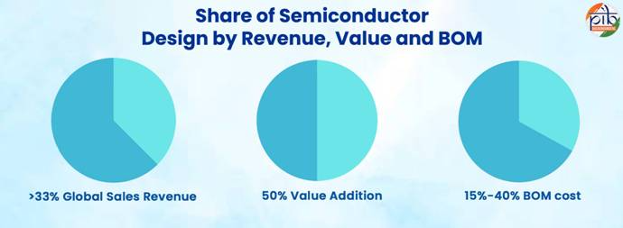
Did You Know: Fabless chip design is the key enabler of semiconductor value chain In the electronics value chain, fabless semiconductor companies hold the highest strategic value because they design the chips that drive product intelligence, efficiency, and security. While fabs manufacture silicon and EMS firms assemble devices, more than half of a semiconductor’s value comes from design and IP, not physical production. Fabless semiconductor design models generate high value addition with relatively modest capital expenditure, as design and IP contribute disproportionately to product economic value. Without strong fabless capability, a nation remains dependent on imported core technologies even if electronics are manufactured locally. Building a robust fabless ecosystem therefore enables India to own the most critical layer of the value chain, retain intellectual property, reduce imports, attract manufacturing, and establish long-term technological leadership. |
DLI Scheme

The Design Linked Incentive (DLI) Scheme is a key instrument in advancing India’s ambition to develop a strong fabless capability. The scheme is implemented by the Ministry of Electronics and Information Technology (MeitY) under the Semicon India Programme to catalyze a strong, self-reliant chip design ecosystem by providing financial incentives and access to advanced design infrastructure for domestic startups and MSMEs.
ELIGIBILITY UNDER THE DLI SCHEME |
Start-ups and MSMEs are eligible for financial incentives and design infrastructure support for semiconductor product design & deployment and other domestic companies are eligible for financial incentives for deploying semiconductor designs.
|
The DLI Scheme supports semiconductor design across the full lifecycle—from design and development to deployment—covering Integrated Circuits (ICs), chipsets, Systems-on-Chip (SoCs), systems and IP cores. By promoting indigenous semiconductor content and intellectual property in electronic products, the scheme aims to reduce import dependence, strengthen supply chain resilience, and enhance domestic value addition.
Financial Incentives and Design Infrastructure Support under DLI
FINANCIAL INCENTIVES | |
Product Design Linked Incentive | Deployment Linked Incentive |
Reimbursement of up to 50% of eligible expenditure.
|
|
| |
DESIGN INFRASTRUCTURE SUPPORT | |
C-DAC has established the ChipIN Centre under the DLI Scheme to facilitate the design infrastructure support to approved companies::
| |
Programme Highlights & Key Achievements of DLI
Since its launch in December 2021, the Design Linked Incentive (DLI) Scheme has been instrumental in shaping a stronger and more self-reliant semiconductor design ecosystem in India. By extending financial incentives, access to advanced design tools, and prototyping support to companies, startups, and academic institutions, the scheme enables innovators to progress seamlessly from ideas to actual silicon chips. This ecosystem-driven approach has been anchored by the creation of shared national infrastructure for chip design.
A key pillar of this infrastructure is the ChipIN Centre, which has democratized access to advanced EDA tools for chip design for about 1 lakh engineers and students across 400 organizations nationwide—making it the world’s largest user base of a centralized chip design facility. This includes support to around 305 academic institutions under the Chips to Start-up (C2S) Programme and 95 startups under the DLI Scheme, significantly reducing entry barriers for early-stage innovators.
Complementing this effort, India’s shared EDA Grid—a national platform offering high-end chip design software—has recorded 54,03,005 hours of cumulative usage by 95 supported start-ups as of 2nd January 2026, reflecting strong adoption by startups, MSMEs, and researchers across all States.
These enabling measures have translated into tangible outcomes for the domestic startup ecosystem. Supported companies under the DLI Scheme have moved from innovation to execution, with ten patents filed, 16 chip-design tape-outs completed, and six semiconductor chips successfully fabricated—marking critical milestones from concept to silicon. In parallel, over 1,000 specialised engineers have been trained or engaged through DLI-supported projects, strengthening India’s design talent base. Beneficiaries have also developed more than 140 reusable semiconductor IP cores, which serve as critical enablers for advanced chip development.
Building on these successes, the DLI Scheme is now driving the transition from design validation to productization, enabling start-ups and MSMEs to move toward volume manufacturing, system integration, and market deployment. This evolving ecosystem not only strengthens India’s domestic semiconductor capabilities but also positions the country as a credible player in global chip design and innovation.
Key Institutional Frameworks for Semiconductor Design
India’s semiconductor ecosystem is being strengthened through a coordinated institutional framework that combines policy leadership, investment support, capacity building, and indigenous technology development. Key programmes and agencies provide end-to-end backing—from incentivizing chip design and manufacturing to developing skilled talent and fostering open-source microprocessor architectures—ensuring India’s progression toward a self-reliant and globally competitive semiconductor design ecosystem.
Initiated at C-DAC, IIT Madras and IIT Bombay has resulted into design, development and fabrication of open-source architecture-based family of microprocessors viz. VEGA12, SHAKTI13 and AJIT microprocessors as a step towards self-reliance.
Together, these institutional initiatives create a robust foundation for India’s semiconductor ambitions, enabling startups, MSMEs, and academic institutions to innovate and scale. By bridging the gap from research to productization, they are driving self-reliance, enhancing global competitiveness, and positioning India as a strategic player in the global semiconductor landscape.
Success Stories of India’s Design Linked Incentive (DLI) Scheme
Under the DLI scheme, 24 chip-design projects have been sanctioned across areas such as video surveillance, drone detection, energy meters, microprocessors, satellite communications, and broadband and IoT SoCs. Additionally, 95 companies have received access to industry-grade EDA tools, significantly reducing design and infrastructure costs for Indian chip design startups. Among the beneficiaries, following companies stands out as leading examples of how the DLI Scheme is nurturing world-class semiconductor innovation:
The success stories illustrate how the DLI Scheme is converting indigenous chip design capabilities into silicon-proven, market-ready products. By supporting advanced design, prototyping, and commercialization, the scheme is strengthening India’s technological self-reliance and its position in the global semiconductor design ecosystem.
Conclusion
The Design Linked Incentive (DLI) Scheme is critical to anchoring India in the most strategic and value-intensive segment of the global semiconductor value chain—chip design. By reducing dependence on imported semiconductor IPs and chips, strengthening resilience against geopolitical and supply-chain disruptions, and ensuring assured access to critical technologies for defence, telecom, AI and mobility, DLI lays the foundation for strategic autonomy and long-term economic growth. The scheme also enables high-value growth by translating deep-tech innovation into globally competitive products, fostering startups and MSMEs, and building a highly skilled engineering workforce.
These outcomes are already evident, with DLI-supported firms achieving multiple chip tape-outs, silicon-proven designs, patents, reusable IPs, trained talent and operational design infrastructure, demonstrating tangible on-ground impact. As the ecosystem enters the productization phase, silicon-validated designs are moving toward volume manufacturing, system integration and market deployment, positioning Indian companies as credible global suppliers while strengthening domestic supply chains and reinforcing India’s self-reliant semiconductor ecosystem.